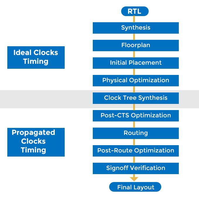
The course is designed for Freshers who want to build their carrier in VLSI domain as Physical design engineer. Training will be delivered by experts in physical design, as per the industry requirements. Importance is given to cover the concepts, methodology with good emphasis on hands-on training, using Industry Standard tools with lab sessions with quality project at the end of the course.
Course Outline:
- CMOS Basics & Physical Design flow
- Design inputs & Sanity Check
- Floor plan and Power planning
- Placement
- Timing Analysis & Optimization (Setup/Hold)
- Clock Tree Synthesis (CTS) and Optimization(Skew, Latency)
- Routing (Different types of routing)
- ECO Flow (Different types of ECO)
- Sign-off Checks (Physical DRC)
- Project

"For training requirement, contact us at This email address is being protected from spambots. You need JavaScript enabled to view it."


